- Thread starter
- #101
First thing to understand about SEM technology is that it's not an optical image that you're seeing. What it is is a topographical map of the surface of your sample. An electron beam is fired at the sample, which excites the atoms on the surface, then these atom give off different energies which the detector in the SEM picks up. The software then makes sense of the data and draws the map that you see. The advantages of technology is that you can see detail to nearly the atomic scale, the disadvantages are that you sample needs to be conductive to work in a traditional SEM and that depending on the surface make-up, details you see optically, may not show up in the SEM.
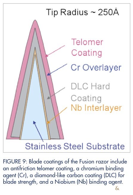
Teflon is easy to spot because it's not conductive and will charge (basically, bounce back all the electrons shot at it). Charging particles will turn a brilliant white color in the SEM. The Gillette's don't appear to be Teflon coated, but may have a chrome coating or similar which will excite similarly to the stainless base and make it harder to distinguish in the SEM scan.
I'm learning a lot in this process and may revisit the first set of blades when I get time. It would be interesting to see if my improved technique changes what I initially recorded.
--Edit--
Also, what's the magnification factor of the USB microscope. The SEM images are at 150x and we're looking at a much smaller section of the edge. The roughness may smooth out as we get a closer look.
Last edited: